从本文开始,将正式介绍VitisAI的工作流程。第一个流程就是Vivado Flow,在Vivado开发环境中创建一个硬件平台,最终的输出是xxx.xsa硬件描述文件,为后续的PetaLinux和Vitis提供基础。Vivado中的大部分的内容都是在Block Design中完成的,核心目标是创建一个Zynq UltraScale MPSoC的运行硬件环境,以及为DPU的正常运行提供硬件支持。这里需要注意,较老版本的VitisAI教程中,需要在Vivado中导入DPU的IP核,这种做法已经成为历史,本文介绍的流程中,在Vivado中是不需要导入DPU IP核的,只是对DPU运行环境进行支持,例如中断、时钟等
创建Vivado工程
打开vivado
1 | source /opt/pkg/xilinx/Vivado/2021.1/settings64.sh |
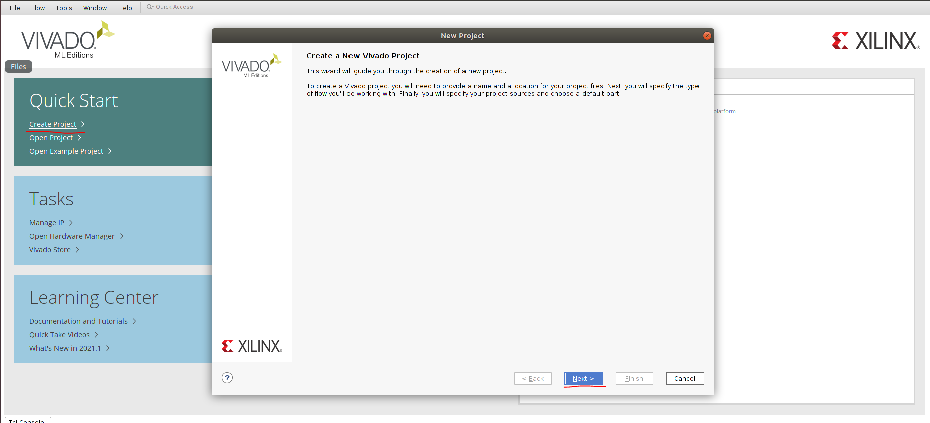
vivado打开后,点击Create Project->Next
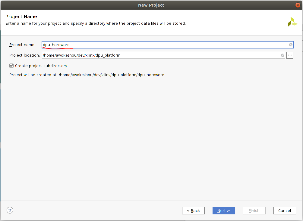
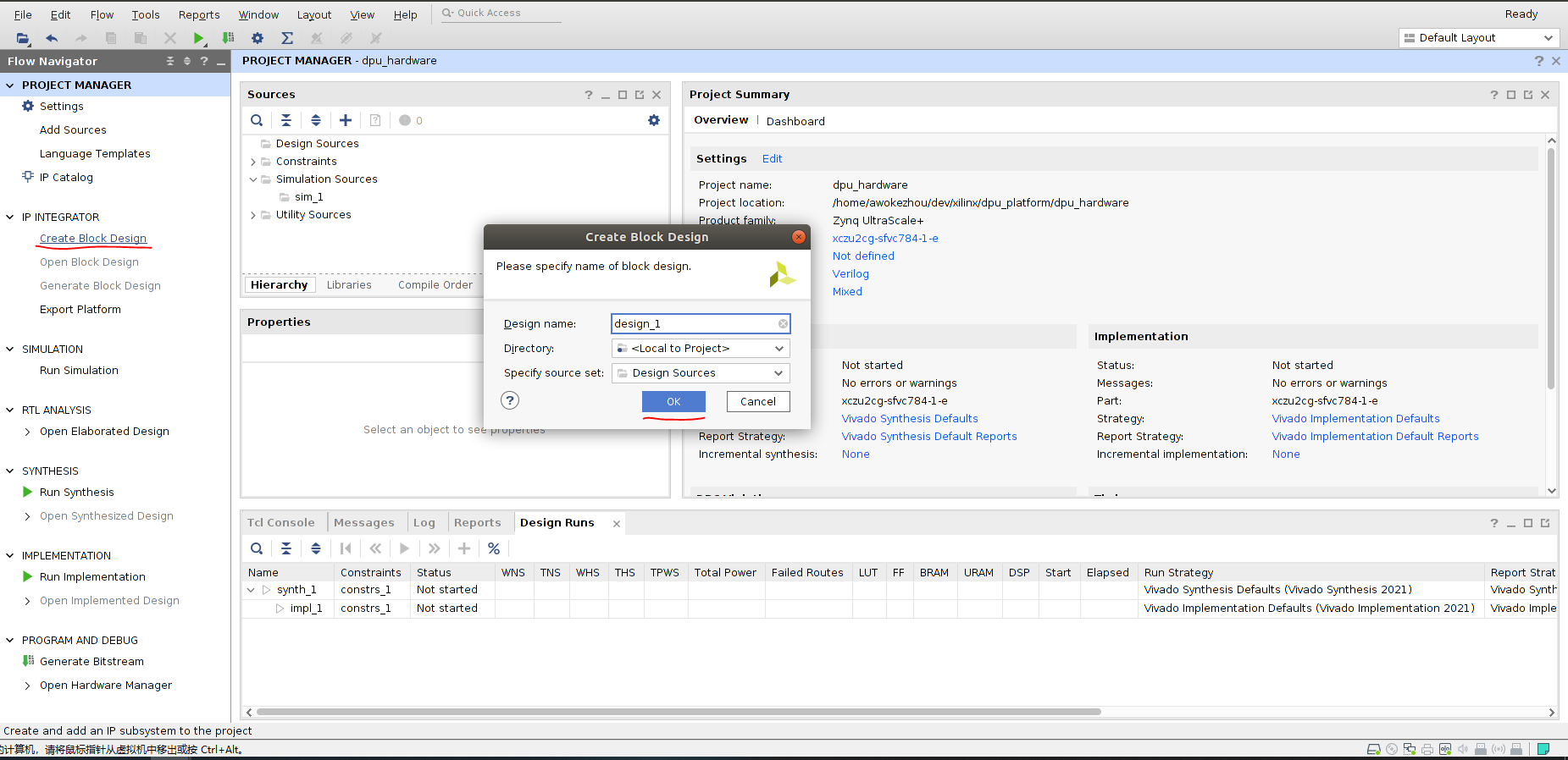
输入项目名称,这里我输入的是”dpu_hardware”,点击Next
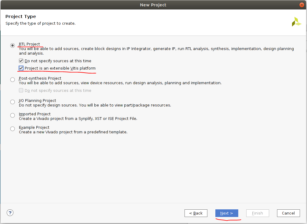
在Project Type页面中选中RTL Project,并选中Project is an extensible Vitis platform,点击Next
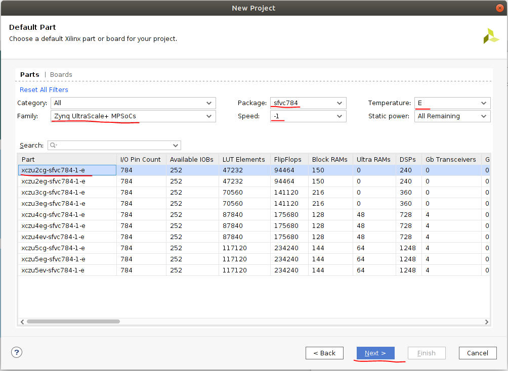
在Default Part页面选择Family为Zynq UltraScale+ MPSoCs,Package为sfvc784,Temperature为E,Speed为-1,并在下方的表格中选中xczu2cg-sfvc784-1-e,点击Next,再点击Finish。这里需要注意,读者的芯片类型选择需要和自己的板子匹配
Block Design IP核添加
在左侧PROJECT MANAGER→IP INTEGRATOR点击Create Block Design,在弹出框中直接点击Next创建一个Block Design
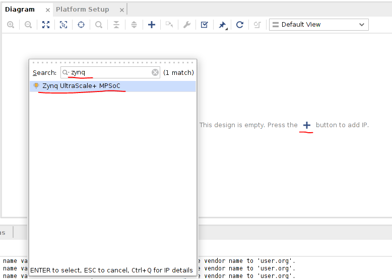
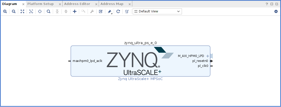
在Diagram界面中点击加号,在搜索框中输入zynq,选择Zynq UltraScale+MPSoC,将其添加到Block Design中
添加后如下图所示
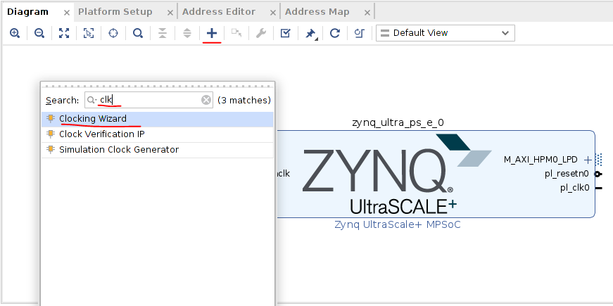
添加Clock
添加Clocking Wizard IP核
添加后如下图所示
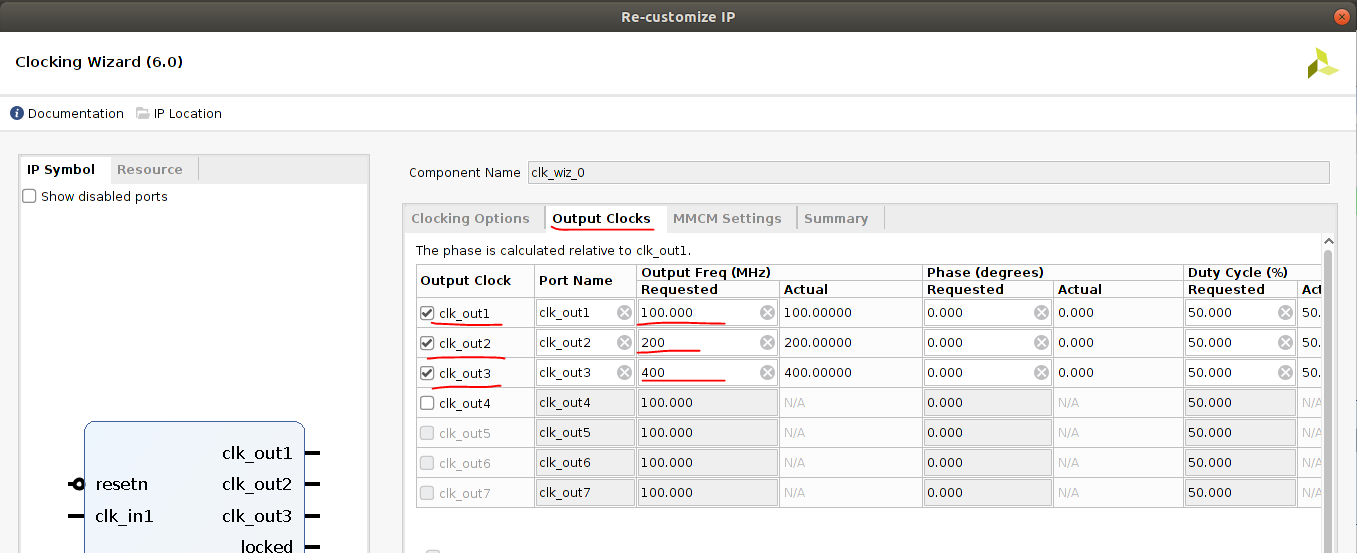
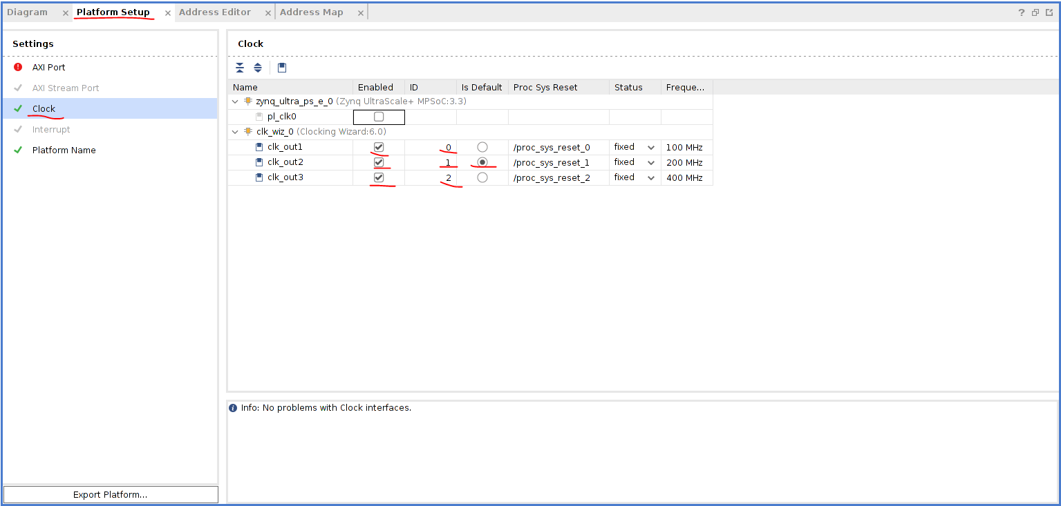
双击Clocking Wizard进入配置页面,在Output Clocks中选中clk_out1、clk_out2、clk_out3,并将Output Freq分别设置为100、200、400
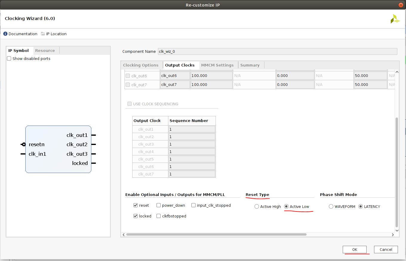
在Reset Type中选择Active Low,并点击OK
添加Processor System Reset
添加Processor System Reset
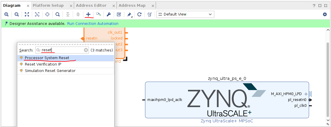
因为有3路时钟,因此要创建3个对应的Reset模块,可点击添加的Reset,Ctrl+C/Ctrl+V复制2个出来
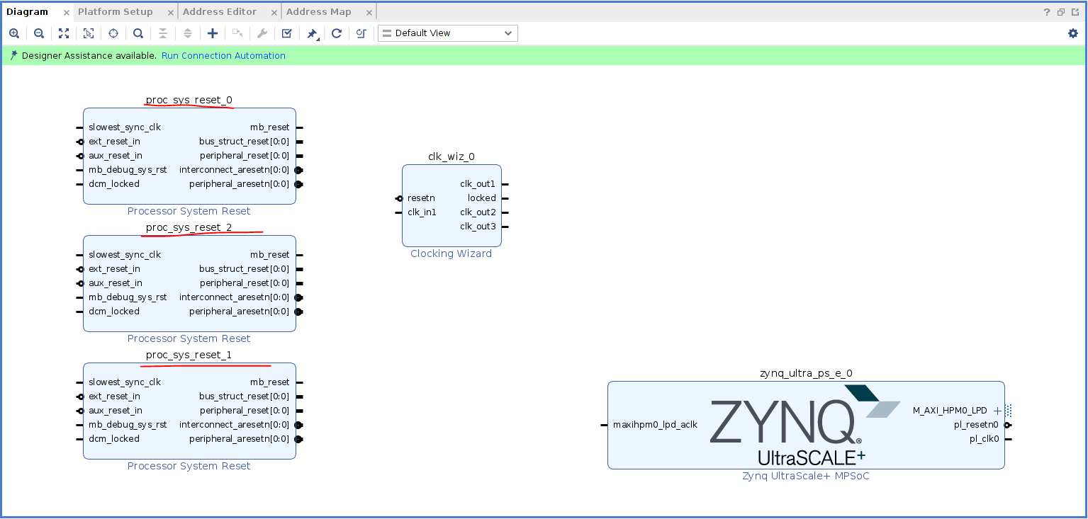
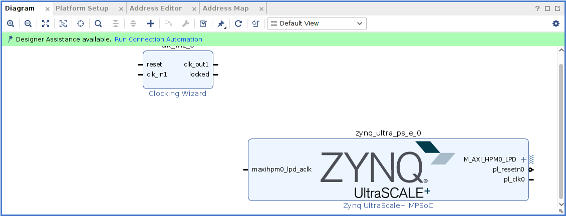
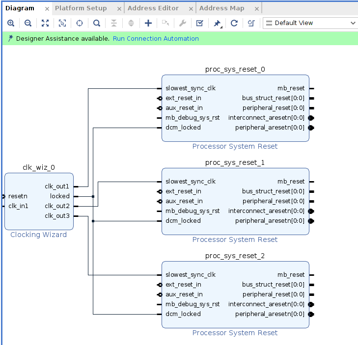
将Clocking Wizard的3路输出分别与Reset0/1/2的slowest_sync_clk管脚相连,将Clocking Wizard的locked与3个Reset的dcm_locked都相连
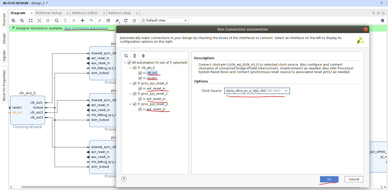
点击Run Connection Automation,在弹出框中将clk_in1选择为zynq的clk0,将3个reset都选择为zynq的resetn0,点击OK
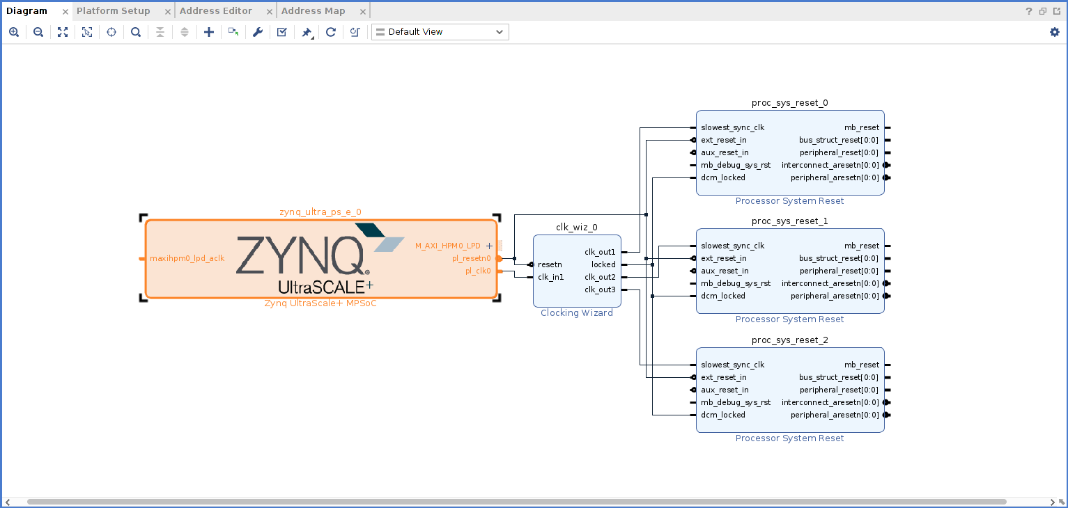
完成后Block Design如下图
点击Platform Setup,选中Clock,将3个Clock都设置为Enable,ID号分别设置为0、1、2,并将clk_out2设置为default
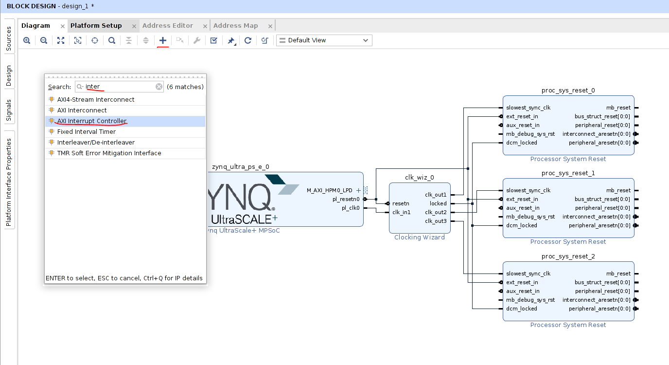
添加AXI Interrupt Controller
添加AXI Interrupt Controller IP核
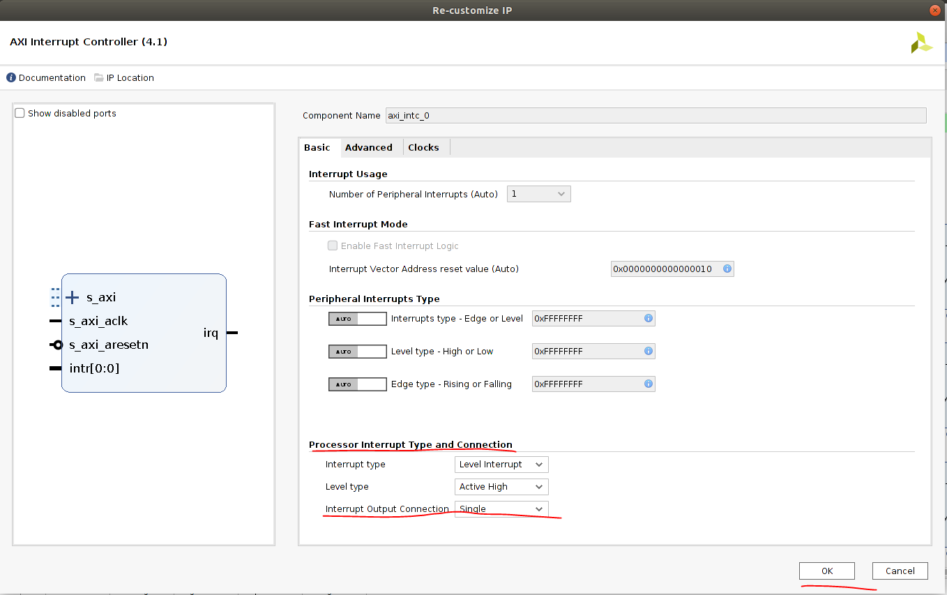
双击AXI Interrupt Controller进入配置页面,将Interrupt Output Connection选择为Single,点击OK
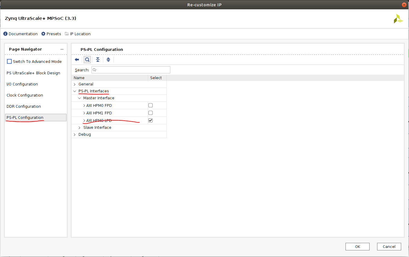
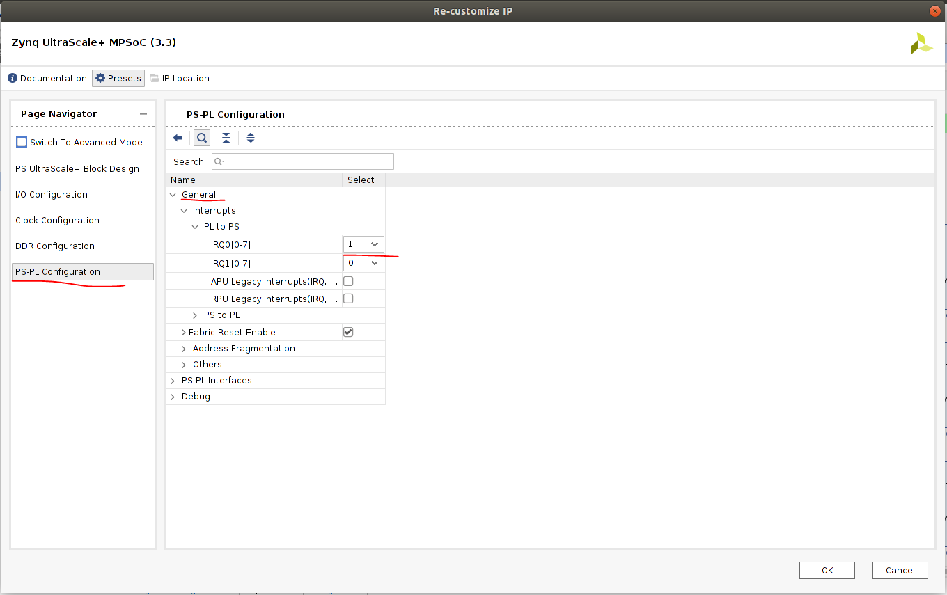
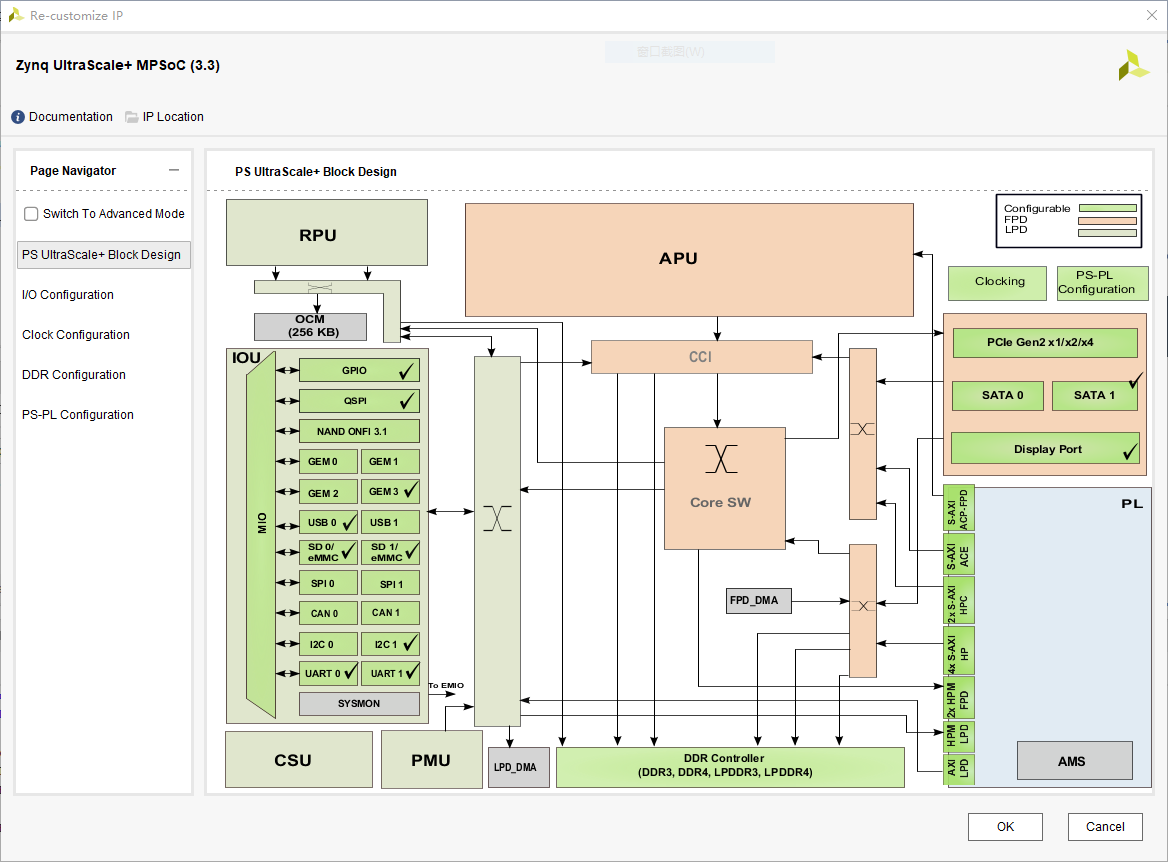
双击ZYNQ进入配置页面,在PS-PL Configuration→PS-PL Interfaces→Master Interface中,确保两个FPD未选中,LPD选中
在PS-PL Configuration→General→Interrupts→PL to PS中,将IRQ0[0-7]选择为1,点击OK
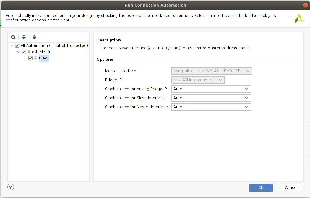
点击自动连接,默认都选择auto,点击OK
整个Block Design如图
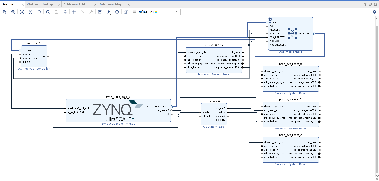
将axi_intc_0的irq连接到ZYNQ的pl_ps_irq0上,再点击图标刷新画布
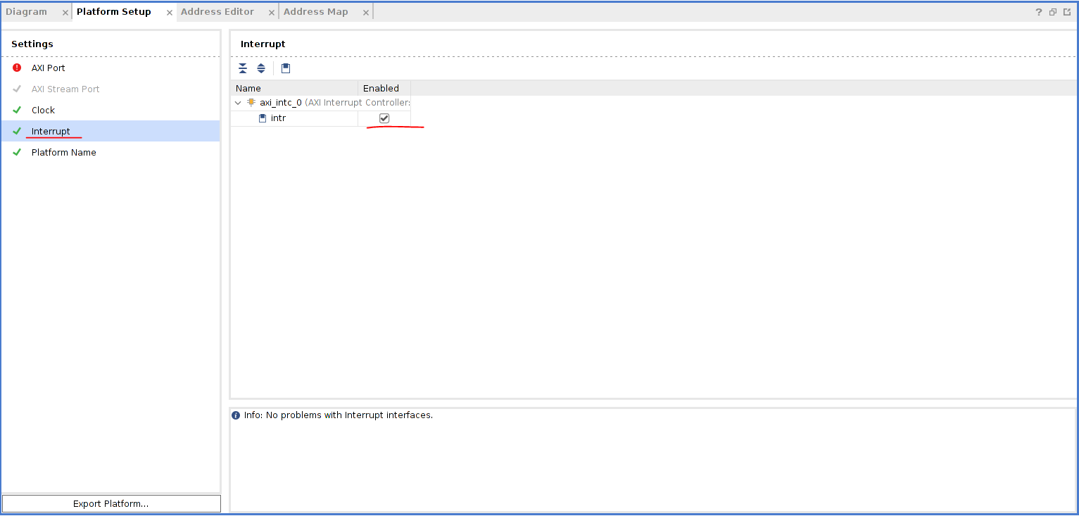
在Platform Setup中将中断使能
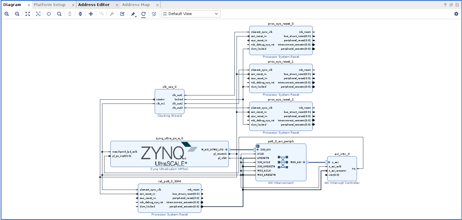
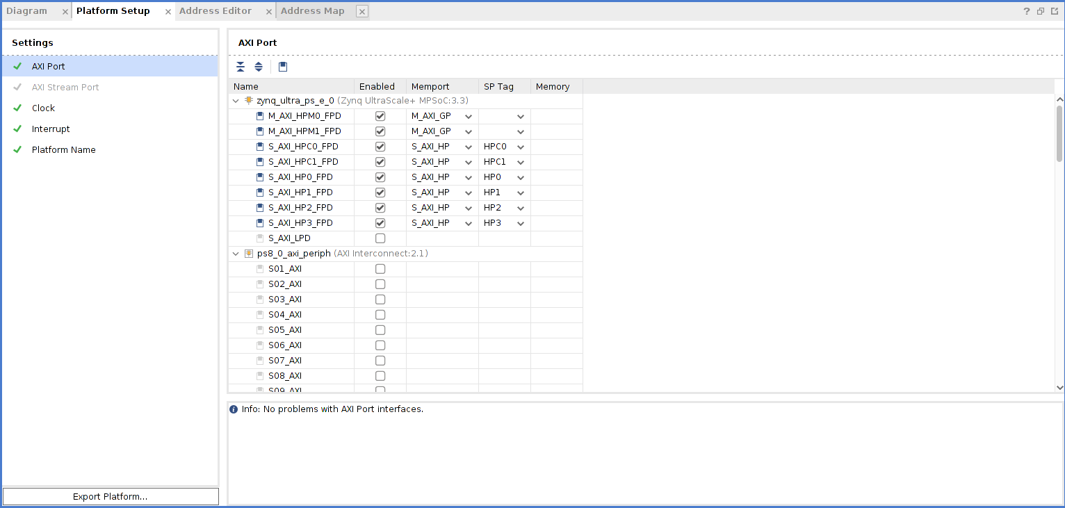
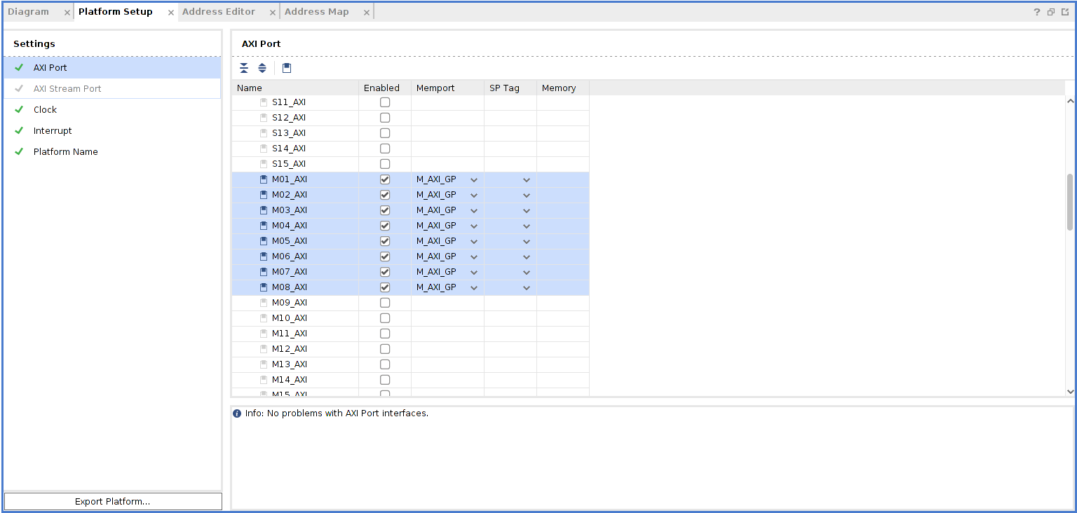
选择AXI Port,按照下图对端口进行配置
Zynq SoC配置
双击Zynq UltraScale MPSoC,打开其配置界面
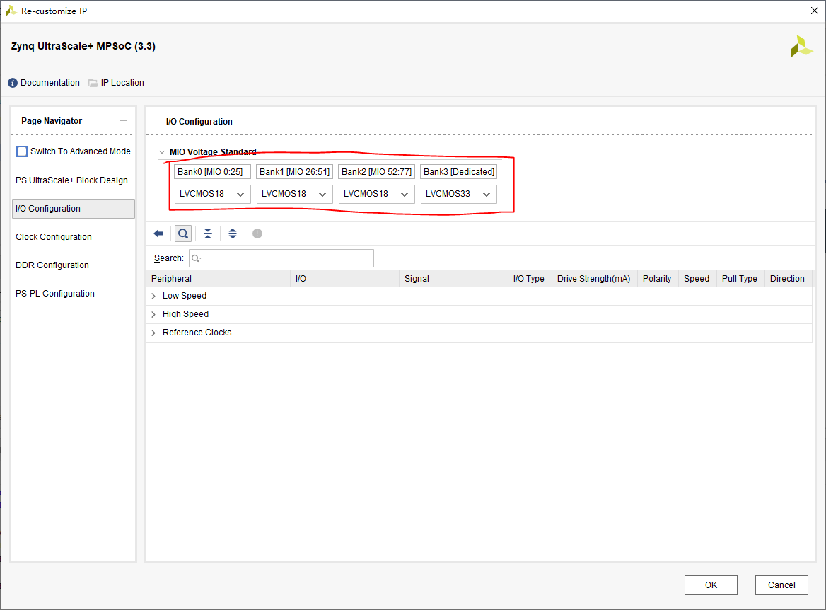
I/O配置
在I/O Configuration中,配置Bank0~Bank2电压为LVCMOS18,Bank3电压为LVCMOS33
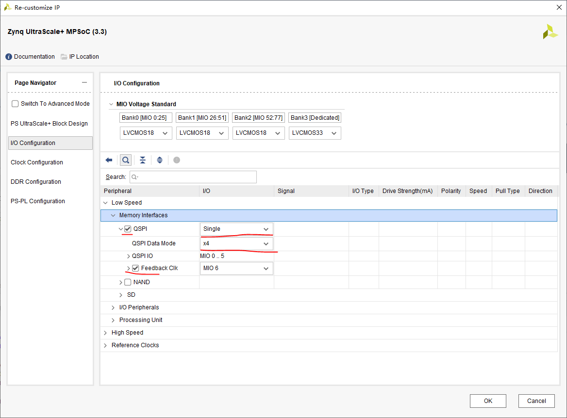
在下方展开Low Speed→Memory Interfaces→QSPI,勾选QSPI,设置模式为Single,Data Mode选择x4,勾选Feedback Clk
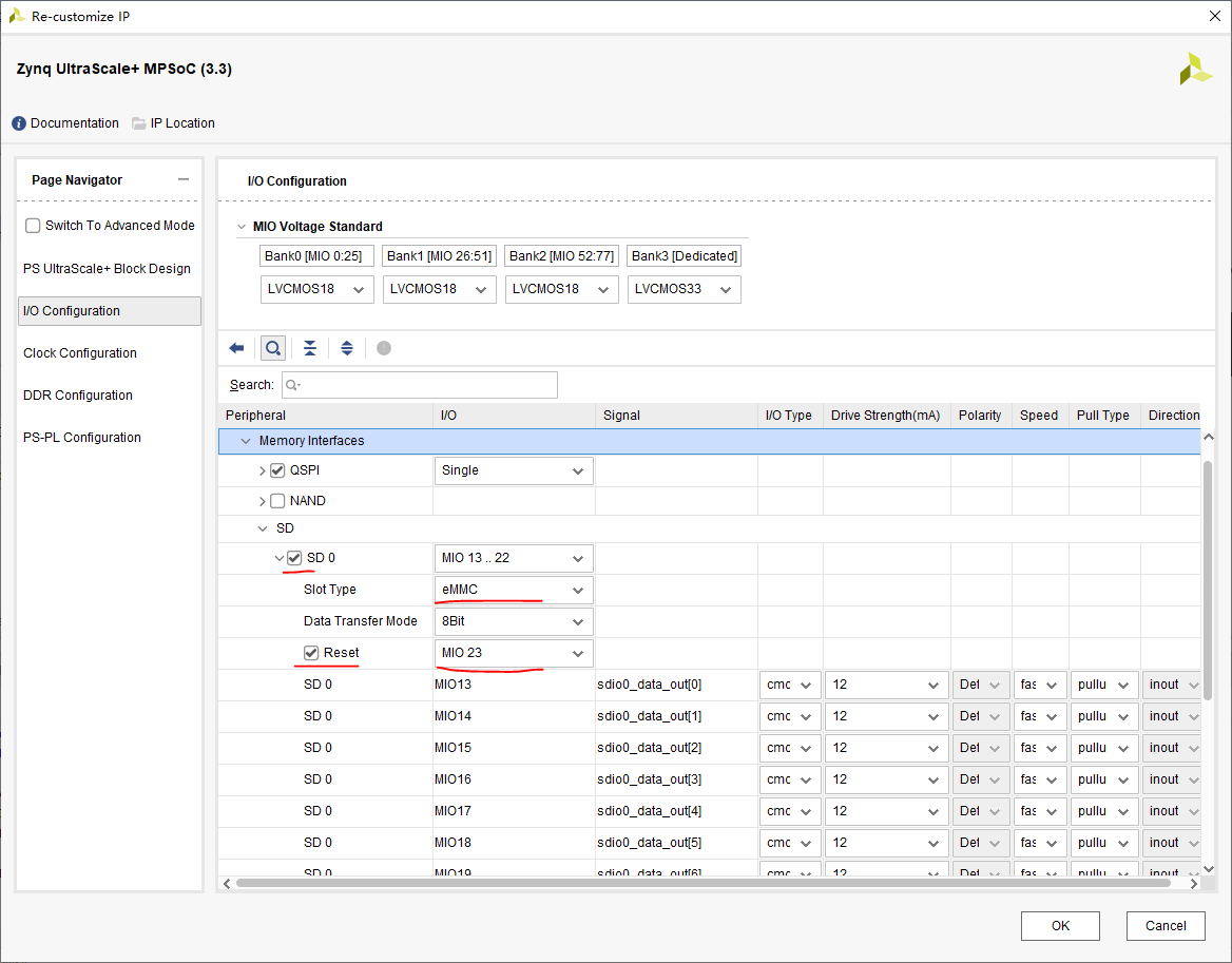
展开SD,并勾选SD0,配置Slol Type为eMMC,Data Transfer Mode为8Bit,勾选Reset,选择MIO23
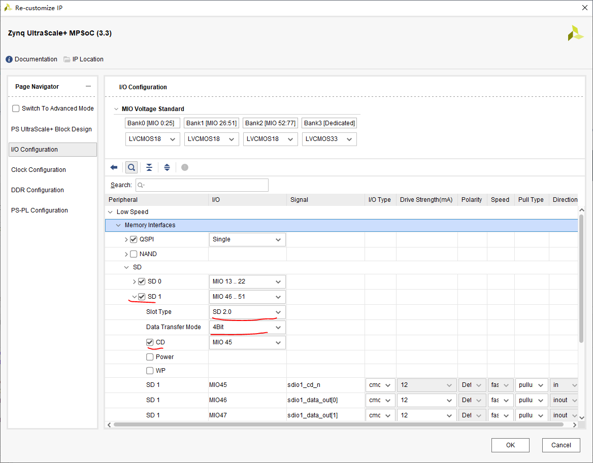
勾选SD1,Slot Type选择SD 2.0,Data Transfer Mode选择4Bit,勾选CD,用于检测SD卡的插入
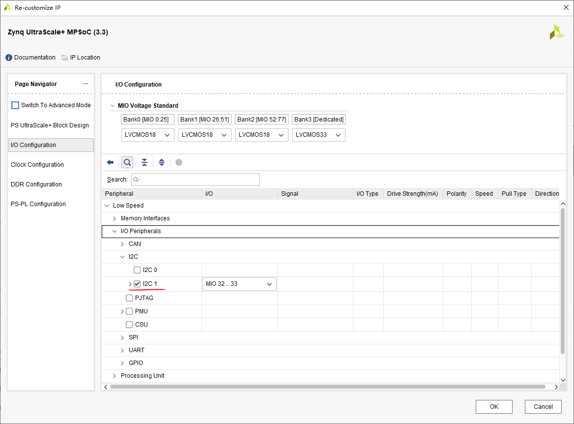
勾选I2C 1,用于EEPROM
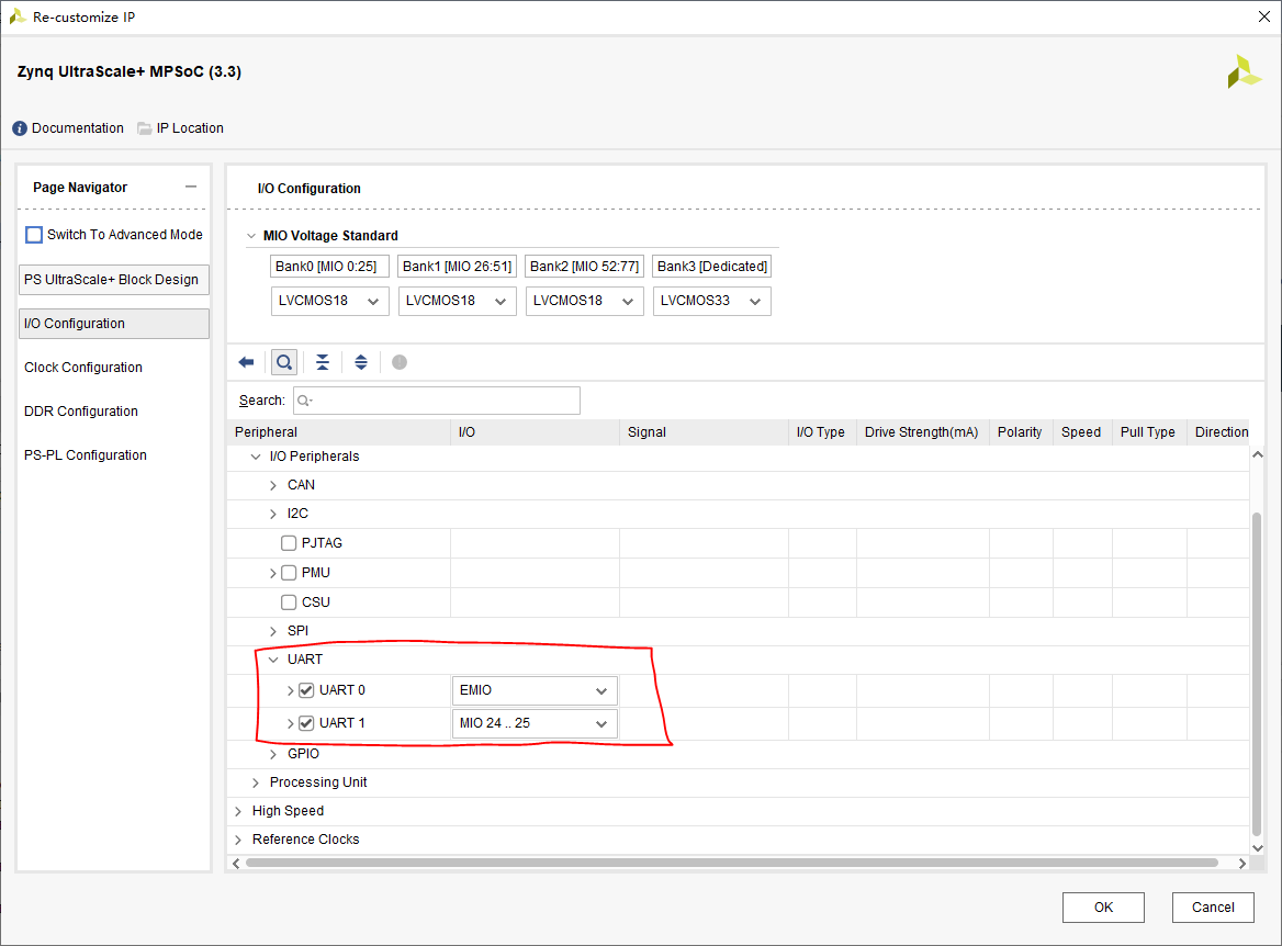
勾选UART1
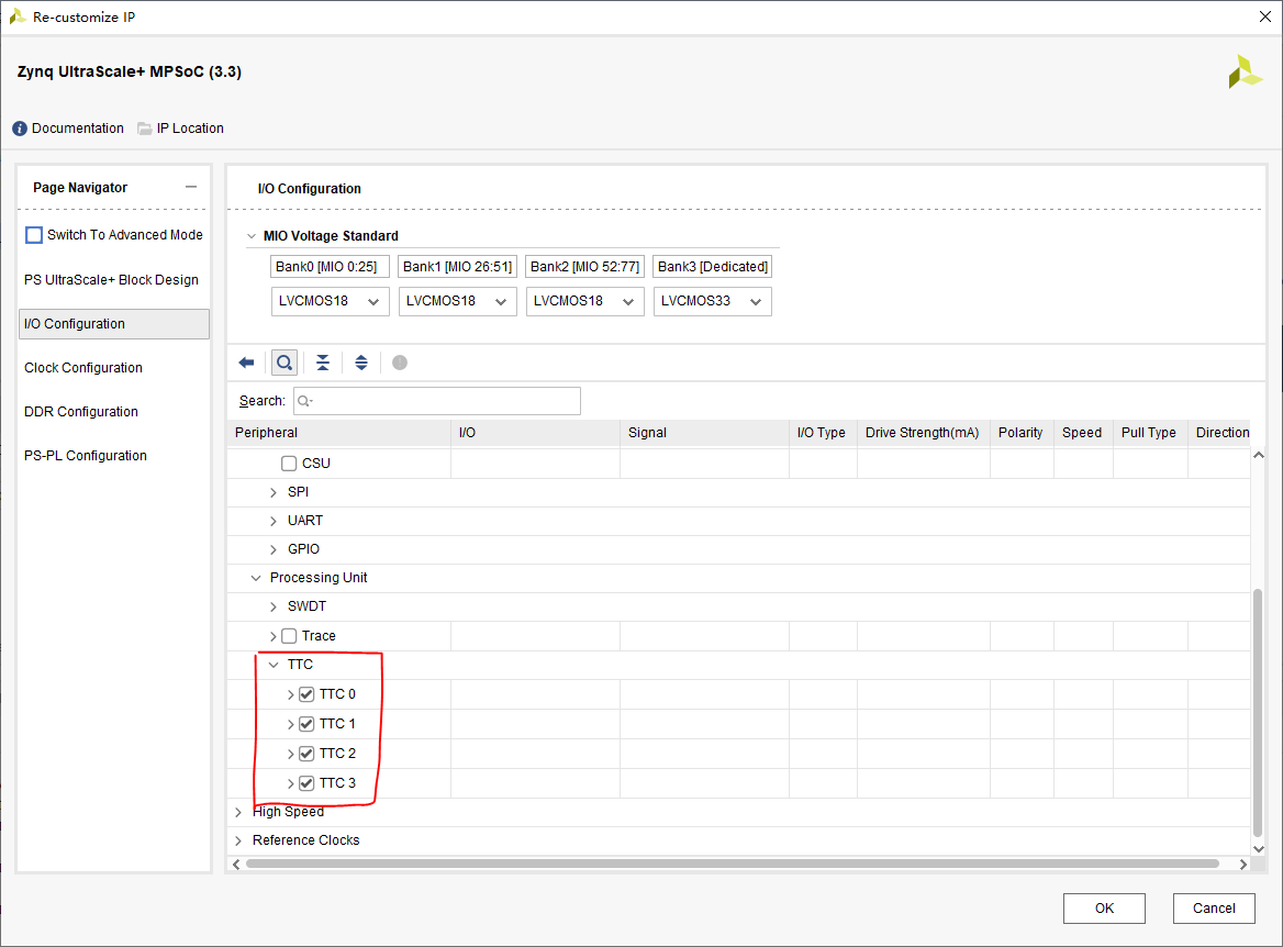
勾选TTC 0~TTC3
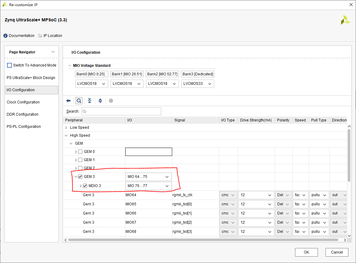
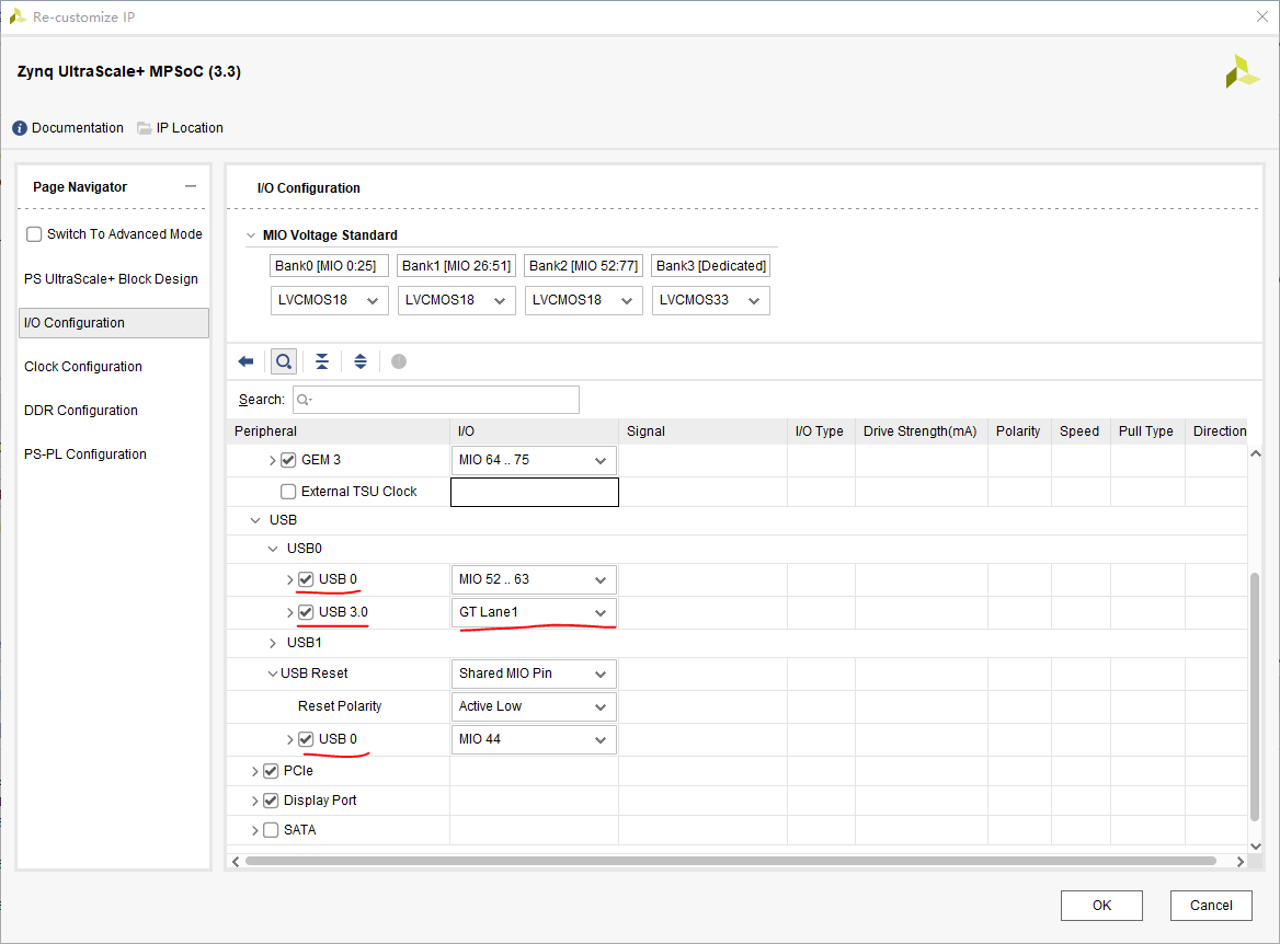
配置PS端以太网,勾选GEM3,勾选MDIO3
勾选USB0,勾选USB3.0,选择GT Lane1,勾选USB Reset→USB 0
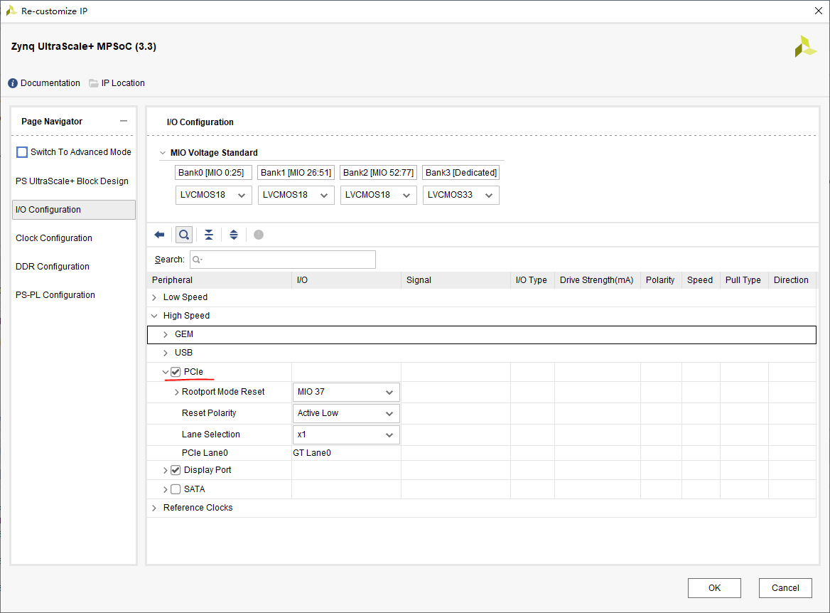
勾选PCIe
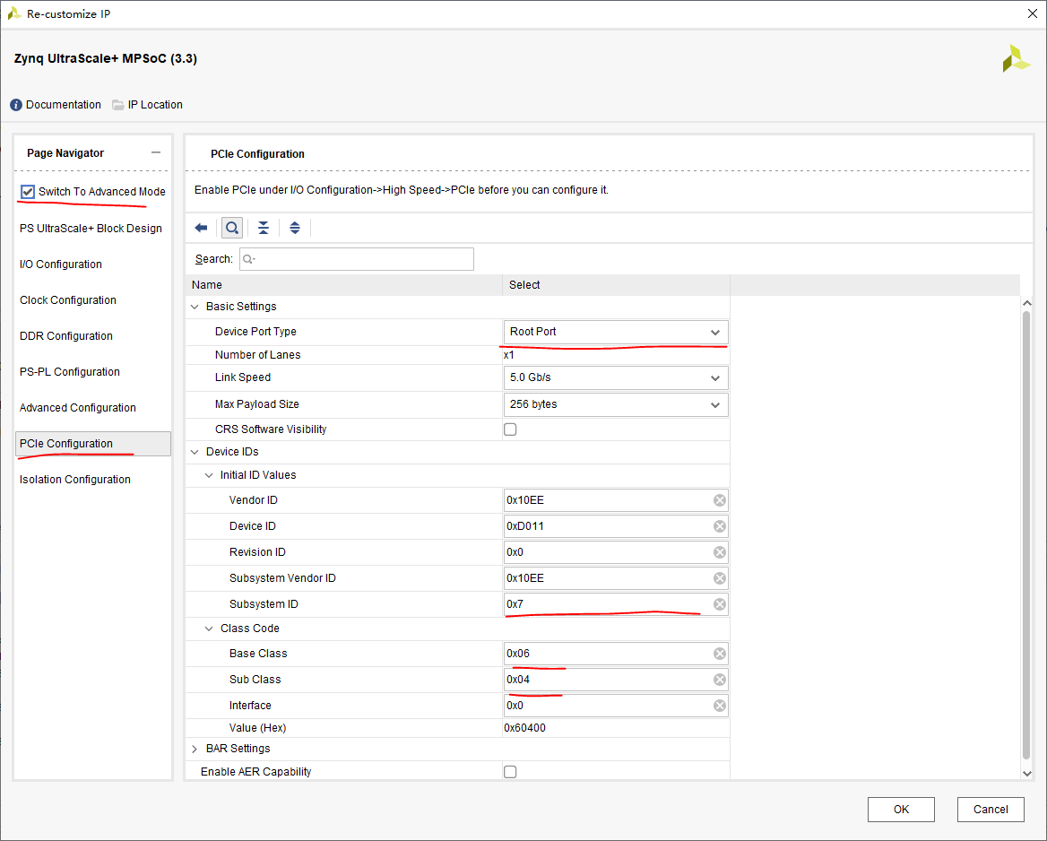
点击左侧Switch To Advanced Mode,选择PCIe Configuration
- Basic Settings→Device Port Type:RootPort
- Devices IDs→Initial ID Values→Subsystem ID:0x7
- Devices IDs→Class Code→Base Class:0x06
- Devices IDs→Class Code→Sub Class:0x04
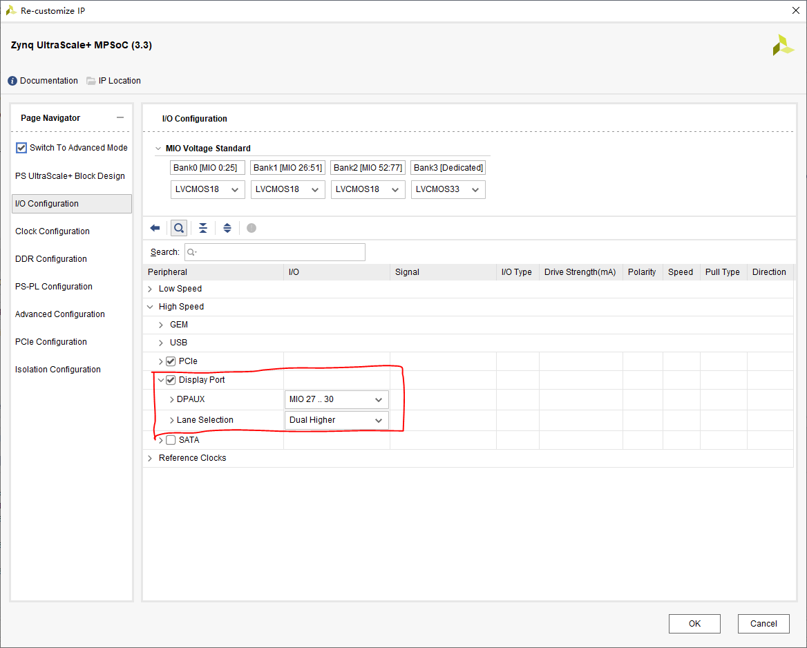
回到I/O Configuration,勾选Display Port,Lane Selection选择Dual Higher
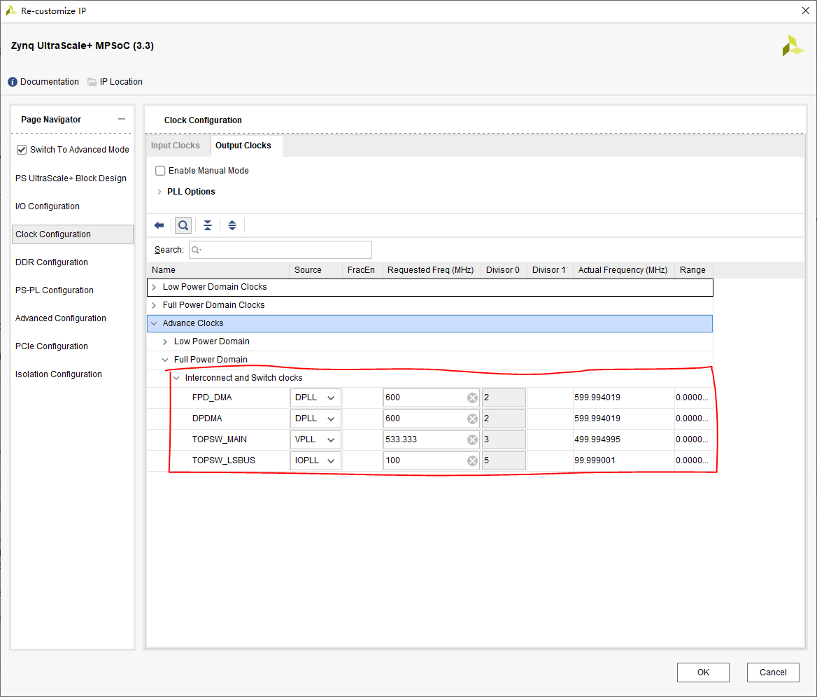
时钟配置
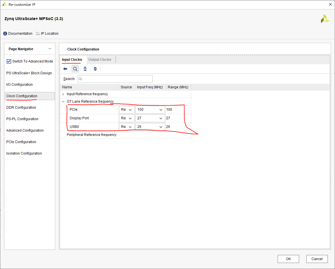
在Clock Configuration界面,Input Clocks配置参考时钟,PCIe选择Ref Clk0,100MHz,Display Port选择Ref Clk2,27MHz,USB0选择Ref Clk1,26MHz
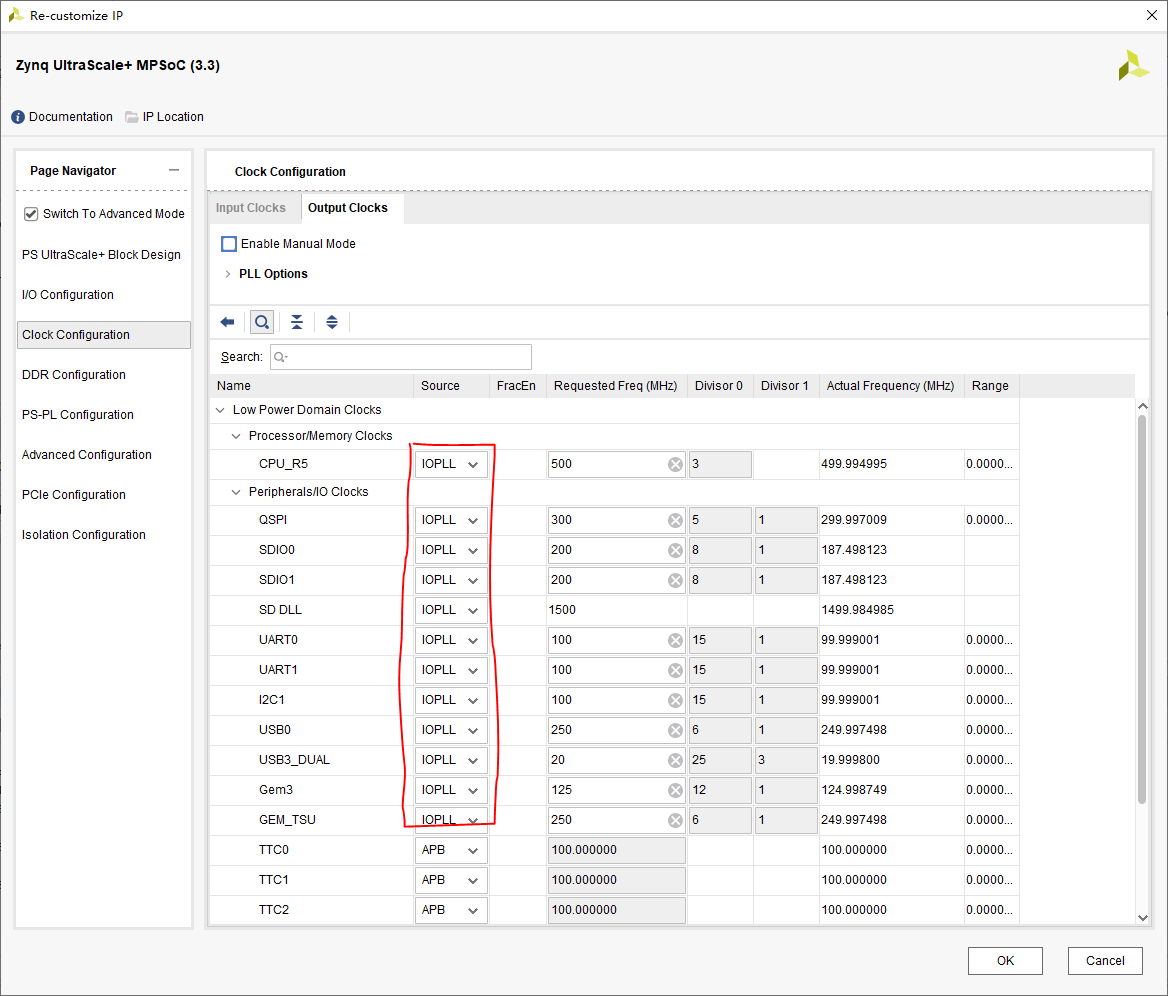
在Output Clocks窗口,如果不是IOPLL,改为IOPLL,保持一致
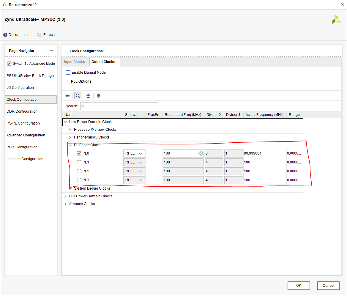
PL的时钟保持默认
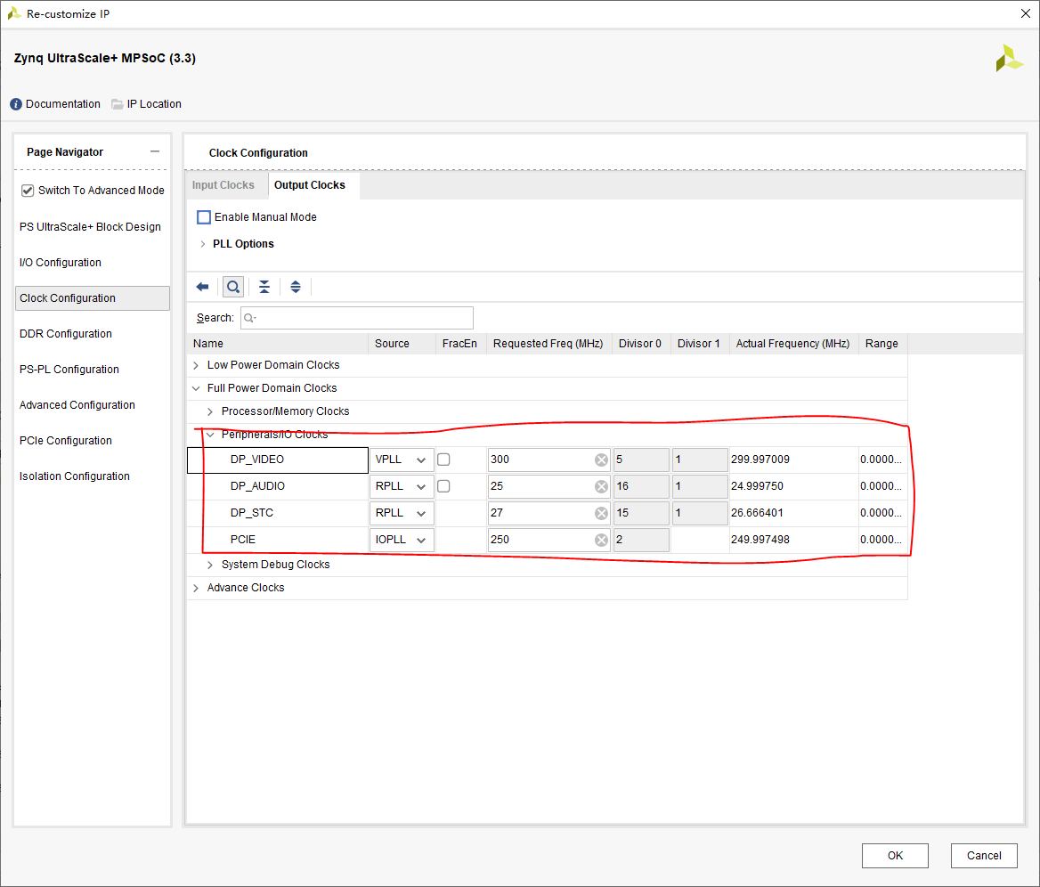
Full Power部分,其他保持默认,将DP_VIDEO改为VPLL,DP_AUDIO和DP_STC改为RPLL
最下面的Interconnect修改如下
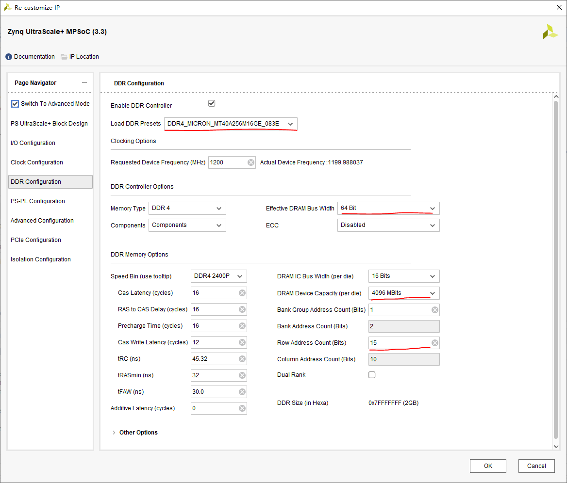
DDR配置
在DDR Configuration窗口中,Load DDR Presets选择“DDR4_MICRON_MT40A256M16GE_083E”
生成bit
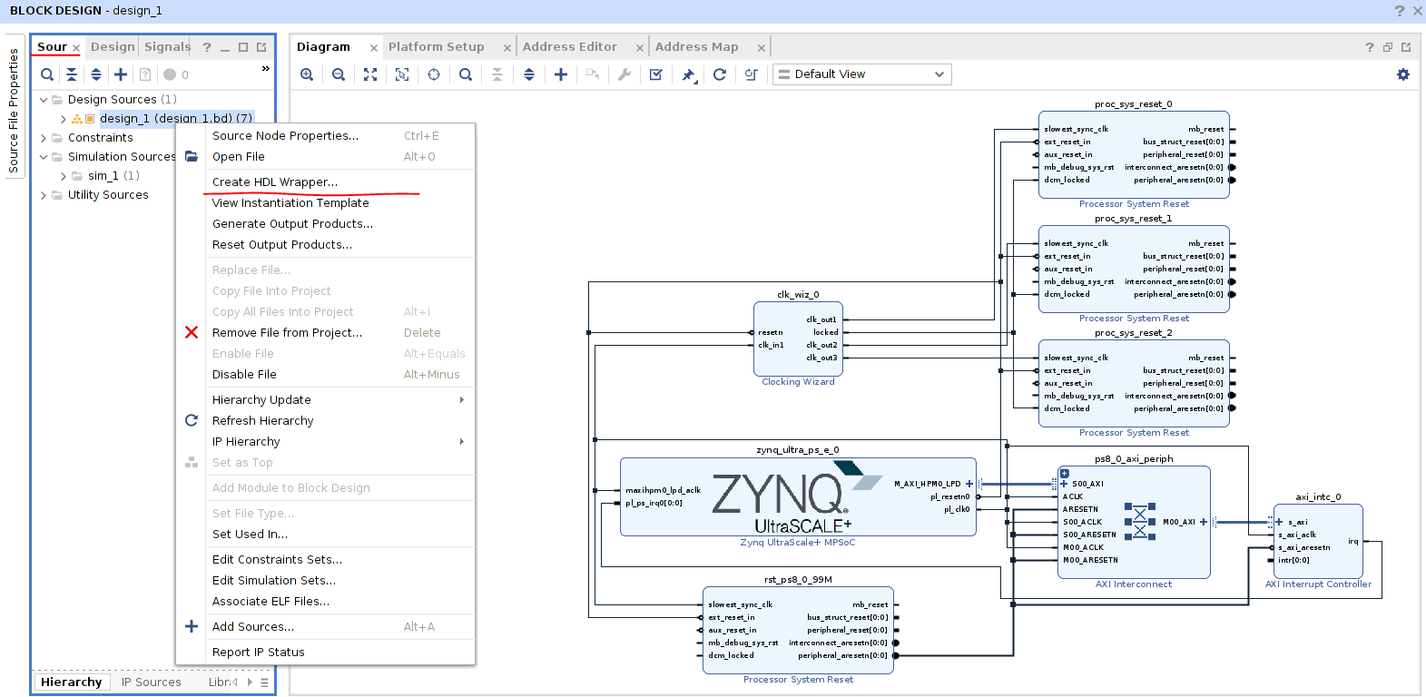
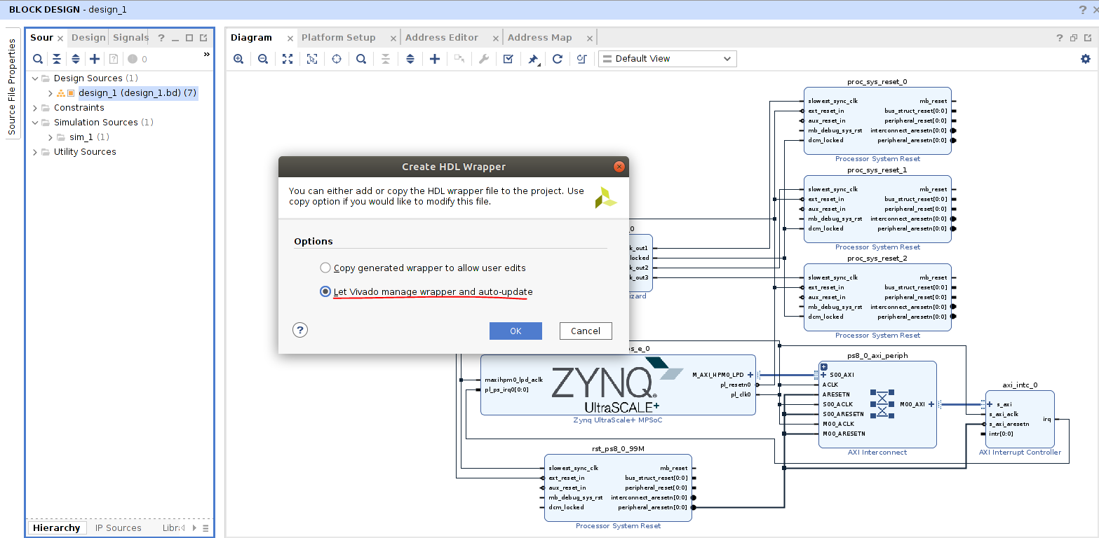
BLOCK DESIGN→Sources→design_1,右键选择Create HDL Wrapper生成top文件
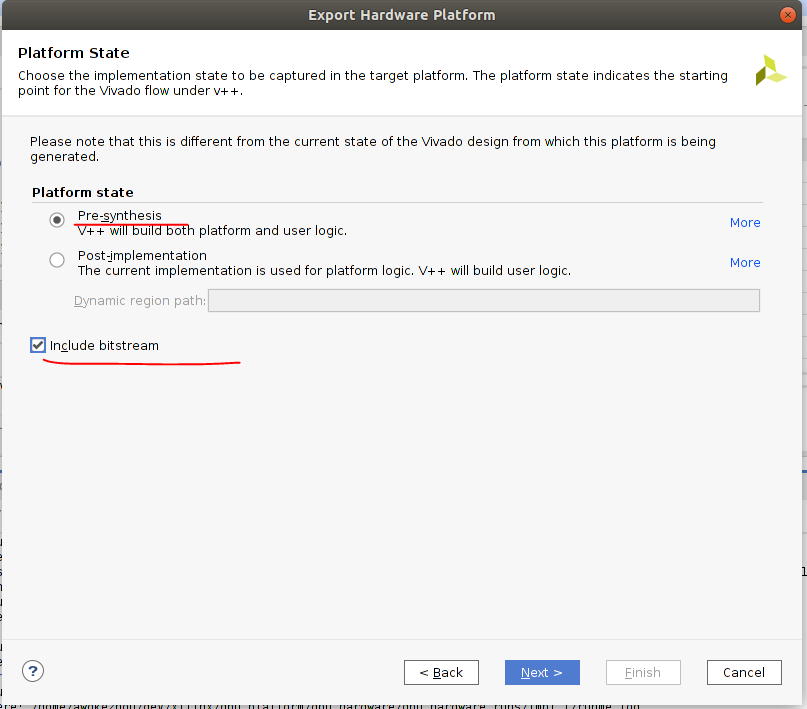
点击Generate Bitstream图标生成bit流,等待生成完成后,点击File→Export→Export Platform,选Next、选Hardware。选Pre-synthesis+include bitstream
设置平台名称等信息,点击Next、Finsih,可看到在dpu_hardware路径下生成了design_1_wrapper.xsa文件